India’s semiconductor ambitions have shifted into high gear with the transition to Semiconductor Mission 2.0 (ISM 2.0) as of April 2026.
For decades, India was known as the world’s back office for software design. As of April 2026, India’s semiconductor strategy has intensified, transitioning into Semiconductor Mission 2.0 (ISM 2.0). This marks a shift from preliminary planning to rapid ecosystem expansion, underpinned by a significant new financial investment from the government.
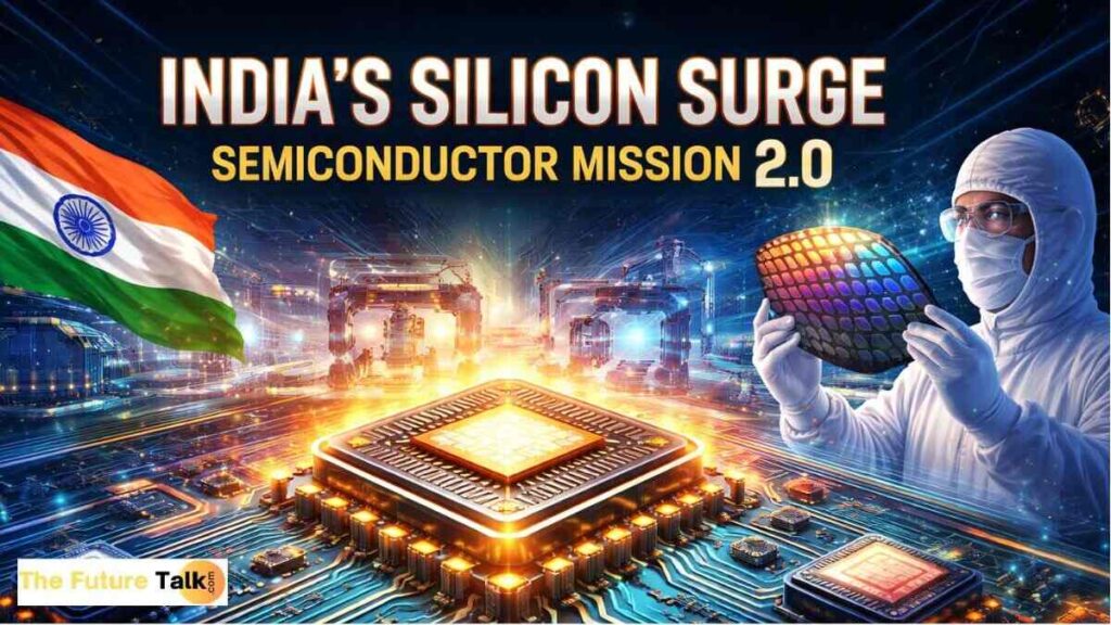
India Semiconductor Mission 2.0 (ISM 2.0)
The Finance Ministry has reportedly sanctioned Rs 1.20 lakh crore (approx. $14.5 billion) for ISM 2.0, building upon the successful outcome of the program’s initial phase.
The second phase of the India Semiconductor Mission (ISM 2.0), currently awaiting final Union Cabinet approval expected by mid-April 2026, marks a significant shift in focus. Unlike the initial phase (ISM 1.0), which primarily aimed at attracting fabrication units (fabs), the new strategy targets highly specialized areas:
- Advanced Manufacturing: Focusing on next-generation technology, specifically 3-nanometre and 2-nanometre nodes.
- Upstream Supply Chain Localization: Promoting domestic production of essential components, including specialized chemicals, gases, and semiconductor manufacturing equipment.
- Intellectual Property and Design: Offering incentives to foster domestic chip design capabilities and the creation of Indian-owned intellectual property.
Also Read: Top 10 Green Data Center Companies in India and World
Key Plant Openings & Operational Milestones
The government of India demonstrated a rapid “one plant per month” inauguration rhythm in early 2026 for its semiconductor manufacturing initiative:
- February 2026: Micron Technology (Gujarat) began commercial production on February 28. This facility is responsible for the assembly and testing of DRAM and NAND products.
- March 2026: Kaynes Semicon (Sanand, Gujarat) was inaugurated by Prime Minister Narendra Modi on March 31. This Outsourced Semiconductor Assembly and Test (OSAT) plant is already supplying Intelligent Power Modules to clients in Silicon Valley.
This pace is expected to continue, with two additional plants scheduled for later in 2026 (one starting in July), bringing the total number of operational semiconductor units to four by the end of the year.
Major Ongoing Projects
Across four states, the government has given approval for 10 major projects, representing a total investment of Rs 1.6 lakh crore.
| Project / Company | Location | Investment | Capacity / Focus |
| Tata Electronics & PSMC | Dholera, Gujarat | Rs 91,526 Cr | First major Fab; 50,000 wafers/month; 28nm nodes. |
| Tata Electronics (OSAT) | Jagiroad, Assam | Rs 27,120 Cr | 48 million units per day; focus on EV and mobile. |
| CG Power & Renesas | Sanand, Gujarat | Rs 7,584 Cr | Advanced packaging; 15.07 million units per day capacity. |
| Vama Sundari (Foxconn JV) | Uttar Pradesh | Rs 3,706 Cr | Display Driver ICs: 36 million chips per month. |
Other Approved Semiconductor Manufacturing Projects
Kaynes Technology India Limited (KTIL) is establishing a semiconductor manufacturing facility in Gujarat with an investment of Rs 3,307 crores for Wire bond Interconnect, Substrate-Based Packages. The facility will have the capacity to produce more than 6.33 million chips per day.
3D Glass Solutions Inc. (3DGS) in Odisha is establishing a semiconductor manufacturing facility with an investment of Rs 1,943 crores. The plant will handle the assembly of packaged products such as Flip Chip Ball Grid Array (FCBGA) assembly, Radio Frequency System in Package (RF SiP), Antenna in Package System in Package (AiP SiP), glass interposers with passives and silicon bridges, and 3D Heterogeneous Integration (3DHI) modules. The proposed installed capacity for glass panel substrate production, assembly, and 3DHI is around 5800 panels per month, 4.20 million units per month, and 1100 units per month, respectively.
SiCSem Private Limited for a semiconductor manufacturing facility in Odisha with an investment of Rs 2,066 crores. The facility will be set up in a technology partnership with Clas-SiC Wafer Fab Ltd. for SiC fab and Continental Device India Pvt. Ltd. for packaging. The production capacity is 5,000 wafers/month, and the packaging capacity is 8 million units per month.
Continental Device India Private Limited (CDIL) is expanding its semiconductor manufacturing facility in Punjab, with an investment of Rs 117 crores. The facility will manufacture high-power discrete semiconductor devices such as MOSFETs, IGBTs, Schottky Bypass Diodes, and transistors, both in Silicon and Silicon Carbide. The production capacity will be around 158.38 million units/annum.
Advanced System in Package Technologies Private Limited (ASIP) is establishing a semiconductor manufacturing facility in Andhra Pradesh, with an investment of Rs. 480 crores. The facility will be set up in a technology partnership with APACT Co., Ltd., South Korea. The production capacity of the facility would be around 96 million units/annum.
Strategic Initiatives
- Pax Silica: India is now a participant in the U.S.-led Pax Silica initiative, which focuses on guaranteeing secure access to critical minerals and establishing resilient semiconductor supply chains.
- Talent Pipeline: Across 315 universities, nearly 60,000 engineers have received training in global Electronic Design Automation (EDA) tools, including Synopsys and Cadence.
- Design Success: The indigenous Dhruv 64 microprocessor has been developed to provide a secure platform for 5G and industrial automation.
Also Read: AI Superapp: Inside the GPT-5.4
India is strategically positioning itself to become one of the top three global semiconductor nations by 2047. The current decade, termed the “Techade,” is critical, as it will lay the groundwork for the nation’s shift from being primarily a technology consumer to a major global supplier.
Stay tuned to The Future Talk for more such interesting insights. Comment your thoughts and join the conversation.